- APPLY FOR SLOT
- Internal Users
- External Users
- SLOT BOOKING STATUS
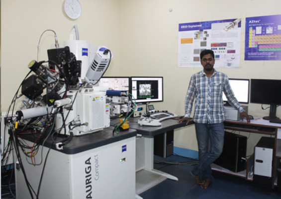
Cross/Dual beam FIB-FEG microscopy Laboratory(FIB Lab)
Phone : +91-3222-282498
Location : NB / GF / 3, CRF
Facilitator :
Prof. Sujoy Kar , Metallurgical & Materials Engineering
Email: sujoy.kar@metal.iitkgp.ac.in, Contact:+91-3222-283258
For Internal Users - Click Here to apply for Slot
For External Users - Click Here to apply for Slot
Objectives
AURIGA Compact FIB-FEG combines with precise milling performance of the Focused Ion Beam (FIB) for nanotomography and nanofabrication with live high resolution (FEG) imaging capability. This microscopy is equipped with in-lens, SESI, BSE, STEM, EBSD, EDS, plasma cleaner, Multi GIS, omniprobe and the local charge compensation (Flood Gun for FIB). TEM sample preparation, nano fabrication with ELPHY Quantum Lithography system and 3D Imaging is the main capability of these instruments.
People

Prof. Sujoy Kar
Facilitator
Metallurgical & Materials Engineering
sujoy.kar@metal.iitkgp.ac.in
+91-3222-283258
Equipment Details
Cross Beam FIB-FEG Scanning Electron Microscope
AURIGATM Compact
Year of installation: 2014
Manufacturer:
Carl Zeiss Microscope GmbH, Germany.
Electron beam column details:
GEMINI-column with 100nA higher current mode. Schottkyemitter type field emission system. 100 v to 30 kV acceleration voltages.
Ion beam column details:
CANION 31 FIB column gallium liquid ion source. Resolution 5.0 nm at 30 kV. Energy range 1 kV – 30kV. Beam or probe current 1 pA – 50 nA.
Utility and Working Principal
Sample Details
Accessories
- BSD-Pneumatic(XB-4QBSD):
The 4QBSD (four Quadrant Backscattered electron Detector) is used to detect backscattered electrons, that have been scattered under very low angle. All sample especially where higher atomic number shows in different contrast. Pneumatic retractable 10mm2 4QBSD - diode. The 4-diode quadrants are independently controlled via dedicated menu allow user to define the topographical and compositional response of the detector. All sample especially where higher atomic number shows in different contrast.
Sample preparation:
• All sample Diameter will be within 10 mm, height will be less than 7 mm.
• Sample should be full dry and need conductive coating for non conductive sample
• Sample surface should be polished.
- STEM-D-PNEUMATIC:
Pneumatic, retractable multi-mode Scanning Tunneling Electron Microscope (STEM) is used to detect electrons for the acquisition of bright-field and dark-field signals that transmitted through an ultrathin specimen like TEM imaging.
Sample preparation:
• Students have to prepare his/her own sample on his/her own TEM copper grid.
- In-lence & SESI Detector:
Combined Secondary Electron Secondary Ion (SESI) detector is used for sample Morphology or Topography image.
Sample preparation:
• All sample Diameter will be within 10 mm, height will be less than 7 mm.
• Sample should be full dry and need conductive coating for non conductive sample
- Multi-GIS:
Multi GIS (Gas injection System) is used to inject 5 different processed gases to the specimen surface for the following application :
- Deposition - Deposit metal and insulator to the sample (Tungsten hexacarbonyl, ethycyclopentadieny platinum, Phenanthrene, carbon and Insulator)
- Gas assisted enhance Etching - enhanced selective etching rate(Xenondifluoride)
- Electron Flood Gun(Specs FG 500) Charge Compensator :
For precise control of the focused ion beam, it is necessary to neutralize the positively charged insulators or semiconductors. The Flood Gun is a low energy electron column providing a high beam current. The electrons are locally distributed on the surface of the sample and neutralize the area exposed to the FIB.
- SMART 3D Reconstruction:
Sample will be etching layer by layer and simultaneously imaged every layer. With SMART 3D Reconstruction application reconstruct 3D image.
Sample preparation:
• All sample Diameter will be within 10 mm, height will be less than 7 mm.
• Sample should be full dry and need conductive coating for non conductive sample
- ELPHY Quantum Lithography system- FIB nanolithography system(RAITH):
With ELPHY Quantum Lithography system (GDSII), we can create and import (Auto CAD - DXF, ASCII, CIF) drawing and lithograph the pattern using ELPHY Quantum Lithography system by FIB. Maximum write field is 175um.
- EDS (X-MaxN 51-XMX1151) OXFORD Instruments:
Energy Dispersive Spectroscopy (EDS) Analysis provides elemental and chemical analysis of a sample using SEM. Different types of analysis like point and id, line scan, Map can be done.
Sample preparation :
• All sample Diameter will be within 10 mm, height will be less than 7 mm.
• Sample should be full dry and need conductive coating for non conductive sample
- EBSD(NordlysMax2 NL04-2412-30) OXFORD Instruments:
EBSD (Electron Backscatter diffraction) is a technique for quantitative microstructure (crystallographic-orientation, texture, phase, grain statistics and strain conditions) analysis. High kV electron fall into 700 tilted sample surface then Electron Backscattered Pattern (EBSP) generate on phosphor screen of EBSD detector, which can be automatically analyzed and indexed. The arrangement of these detected kikuchi bands and arrangement of the houghs peaks directly indicates the orientation of the crystal.
Sample preparation :
• All sample Diameter will be within 10 mm, height will be less than 7 mm.
• Sample should be full dry and need conductive coating for non conductive sample
• Sample should well polish.
• Students should know sample orientation (Rolling direction, Transverse direction and Normal Direction) and available phases information.
- OmniProbe (OP 200):
The Nano manipulator enables efficient in-situ manipulation capabilities that can be integrated into FIB for specially TEM sample preparation.
- Plasma Cleaner:
The Plasma Cleaner Add On is used to generate gas-phase radicals in plasma. This plasma is fully contained in the Plasma Cleaner unit. The radicals migrate into the specimen chamber and chemically react with unwanted hydrocarbons, remove hydrocarbon contamination. In particular, after a plasma cleaning cycle, the specimen surface provides optimal imaging conditions even at very low imaging voltage.
- All sample Diameter will be within 10 mm, height will be less than 7 mm.
- Sample should be full dry and need conductive coating for non conductive sample.