- APPLY FOR SLOT
- Internal Users
- External Users
- SLOT BOOKING STATUS
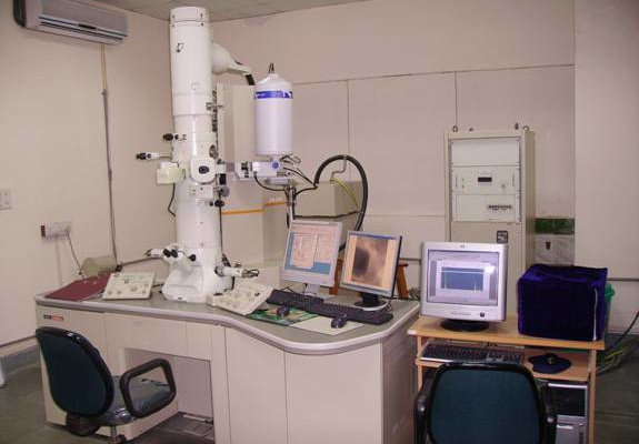
HR TEM Laboratory
Phone : +91-3222-283292
Location : Main Building, CRF
Facilitator :
Prof. Rahul Mitra, Metallurgical & Materials Engineering
Email: rahul@metal.iitkgp.ac.in, Contact:+91-3222-283292
For Internal Users - Click Here to apply for Slot
For External Users - Click Here to apply for Slot
Objectives
- Examination of the microstructure at high resolution
- Identification of phases
- Determination of the crystal structure and orientation of the phases
- Analysis of chemical composition of the individual phases.
People

Prof. Rahul Mitra
Facilitator
Metallurgical & Materials Engineering
rahul@metal.iitkgp.ac.in
+91-3222-283292
Equipment Details
High Resolution Transmission Electron Microscope
Specification of the Instrument:
Specification: JEM – 2100 HRTEM, Make – JEOL, Japan
Point to point resolution - 0.194 nm
Lattice resolution – 0.14 nm
Tilt Angle : 24 ° Acc. Voltage: 200 kV Filament: LaB6
Charge Couple Device (CCD) camera : (Make – Gatan)
Energy Dispersive X-ray (EDX) Analyzer : (Make – Oxford Instruments, U.K)
Manufacturer details:
HRTEM : JEOL Ltd, 1-2, Musashino 3-Chome, Akishima, Tokyo 196-8558, Japan
Charge Couple Device (CCD) camera :Gatan, Inc., 5933 Coronado Lane, Pleasanton, CA 94588, USA
Energy Dispersive X-ray (EDX) Analyzer : Oxford Instruments Analytical, Halifax Road, High Wycombe, Bucks. HP12 3SE, England.
Purchase source (funding): MHRD, GOI
Year of installation: 2006
Utility and Working Principal
The high resolution transmission electron microscope is used to observe the structure and chemistry of electron-transparent crystalline or amorphous specimens, which could be metallic, ceramic, polymeric, or organic in character. The microscope records bright or dark field images, formed by the electron beam either transmitted or diffracted by the periodically arranged atoms, respectively inside a crystalline solid. The images and diffraction patterns contain information on the crystal structure and type of defects present in the solid. Lattice resolution images containing information on atomic-scale structure is obtained from thin crystalline specimens through interference between the diffracted and transmitted beams. Point-to-point resolution of 0.19 nm and line resolution of 0.14 nm are possible under controlled operating conditions. Chemical analysis is possible through detection of characteristic X-rays from different elements in the specimen using the attached Energy Dispersive Spectrometer. The HRTEM provides: (i) Bright and dark field images; (ii) selected area electron diffraction patterns; (iii) convergent beam electron diffraction; (iv) scanning transmission electron microscopy; (iv) Energy Dispersive Spectroscopy.
Sample Details
Samples for HRTEM study should be in the form of circular discs with 3 mm diameter. These could be either self-supported or on a copper grid. For the best results in HRTEM, the samples should have electron transparent area with thickness of around 100 nm or less.
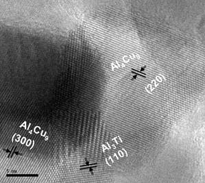
Crystalline intermetallic precipitates of Al4Cu9 and Al3Ti with 40 nm size in an amorphous Al alloy
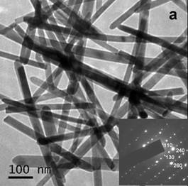
TEM image of BiS3 nano rods TEM image of a nano rod coated with SAED collected from a single nano rod is given in the inset.