- APPLY FOR SLOT
- Internal Users
- External Users
- SLOT BOOKING STATUS
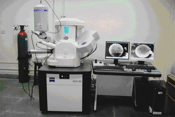
ZEISS Scanning Electron Microscope Laboratory (EVO 60)
Phone : +91-3222-283292
Location : NB / GF / 14, CRF
Facilitator :
Dr. Sujoy Kanti Ghosh, Geology and Geophysics
Email: sujoy.ghosh@gg.iitkgp.ac.in, Contact:+91-3222-283364
For Internal Users - Click Here to apply for Slot
For External Users - Click Here to apply for Slot
Objectives
Scanning Electron Microscope examines the microstructure images and composition analysis (EDS) of surfaces and interphase interfaces of small and of dry specimens.
People
Dr. Sujoy Kanti Ghosh
Facilitator
Geology and Geophysics
sujoy.ghosh@gg.iitkgp.ac.in
+91-3222-283364
Equipment Details
Analytical Scanning Electron Microscope (A-SEM).
ZEISS EVO 60 Scanning Electron Microscope with Oxford EDS Detector. The Microscope works with tungsten filament and maximum acceleration voltage of 30 kV.Facilities:
(1) Secondary Electron Detector (SE),
(2)Backscattered Electron Detector (BSD)
(3) Energy Dispersive X-ray Spectroscopy (EDS): for •Qualitative Microanalysis,
•Quantitative Microanalysis,
•X-ray Area Mapping,
•Line Scanning
(4) Wavelength Dispersive X-ray Spectroscopy (WDS): for
•Qualitative Microanalysis,
•Quantitative Microanalysis
(5) Electron Backscattered Diffraction (EBSD)
(6) Variable Pressure Secondary Electron (VPSE) mode
Manufacturer's details:
SEM: Carl ZEISS SMT, Germany
EDS & WDX: INCA PentaFET x3, Oxford Instrument UK.
EBSD : Nordlys HKL Technology, UK
Sputter coater: POLARON, UK
Purchase source (funding): MHRD
Year of installation: Sept 2008
Utility and Working Principal
Sample Details
The samples should be clean, dry, small piece of solid or powder.