- APPLY FOR SLOT
- Internal Users
- External Users
- SLOT BOOKING STATUS
Hall Effect Laboratory
Phone : +91-3222-283862
Location : NB / FF / 8, CRF
Facilitator :
Prof. Tapan Kumar Nath, Physics
Email: tnath@phy.iitkgp.ac.in, Contact:+91-3222-283862
For Internal Users - Click Here to apply for Slot
For External Users - Click Here to apply for Slot
Objectives
Capable of measuring Hall effect and magneto -resistance measurement of metals, semiconductors etc. in the temperature range of 77 - 300 K in the magnetic field range of -10 kOe - 0 - +10 kOe.
To know temperature dependent Hall mobility, carrier concentration (n), Hall coefficient of doped extrinsic semiconductors - II-VI, group IV, III-V compound semi -conductors etc., it is essential to measure temperature and field dependent Hall resistivity measurements.
To measure ordinary and extra-ordinary Hall resistivity (EHE) of Ferromagnetic materials - especially to know origin of EHE either due to classical Smit scattering or quantum mechanical side jump mechanism this Hall measurement set up is essential. Materials like Fe, Ni, Co, La-Sr-Mn-O3, spintronic materials, Nanometric magnetic materials, Spin Valves, Spin sensors, Magnetic trilayer tunnel juction, Magnetic multilayers semiconducting materials, organic materials etc. are mainly used for Hall and magnetoresistance measurements.
People

Prof. Tapan Kumar Nath
Facilitator
Physics
tnath@phy.iitkgp.ac.in
+91-3222-283862
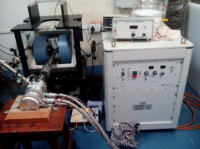
Equipment Details
Hall Effect Measurement set-up
Technique used:
1. Vander Pauw 4 probe electrical Measurement technique in CIP and CPP geometry
2. Hall geometry for Hall measurements.
3. Four probe linear geometry technique.
Manufacturer details: Lakeshore Resistivity and Hall measurement set up.
Purchase source (funding): Institute plan Grant
Year of installation: unknown
Utility and Working Principal
Based on Van der Pauw technique or four probe method and with the help of the 1 Tesla electromagnet along with a liquid nitrogen cryostat assembly one can study Hall Voltage, Hall coefficient, carrier concentration of p-type or n-type semiconducting materials and electronic transport and magneto-transport of various magnetic metals, semiconductors, oxides etc. materials in a form of either bulk or thin film down to liquid nitrogen temperature.
Sample Details
|
Sample Title
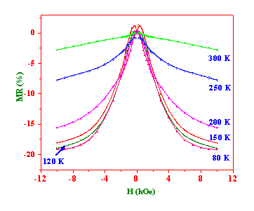
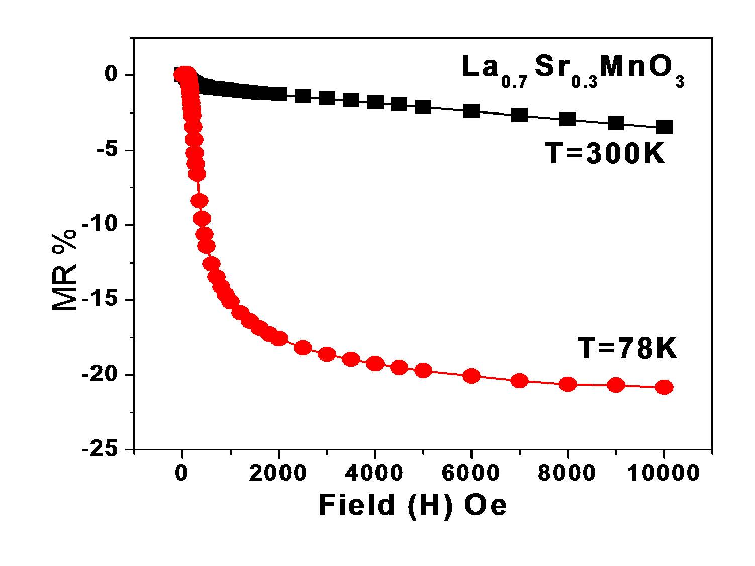
Typical MR curve for a ceramic sample
Sample Title
 |
Typical MR curve for a ceramic sample |
 |
 |