- APPLY FOR SLOT
- Internal Users
- External Users
- SLOT BOOKING STATUS
Field Emission Gun-Scanning Electron Microscope Laboratory (Zeiss Supra 40)
Phone : +91-3222-283288
Location : GF / MME Dept. Room No. 104, CRF
Facilitator :
Prof. Jyotsna Dutta Majumdar, Metallurgical & Materials Engineering
Email: jyotsna@metal.iitkgp.ernet.in, Contact:+91-3222-283288
For Internal Users - Click Here to apply for Slot
For External Users - Click Here to apply for Slot
Objectives
Electron Microscopes are indispensable tools for today's nano technology,development and production. Field Emission Gun Scanning electron microscopes (FEG-SEM) deliver high resolution surface information and are widely used in many application fields such as:
- Materials analysis
- Life Science
- Semiconductor technology
- Quality assurance
The addition of analytical detectors enables full nano structural analysis. The SUPRA™ series, based on the 3rd generation GEMINI® column, offers a complete range of ultra high resolution FE-SEM models to cover all fields of applications in nano technology, cryo, nano structural materials analysis and semiconductor development and failure analysis.
People

Prof. Jyotsna Dutta Majumdar
Facilitator
Metallurgical & Materials Engineering
jyotsna@metal.iitkgp.ernet.in
+91-3222-283288
Equipment Details
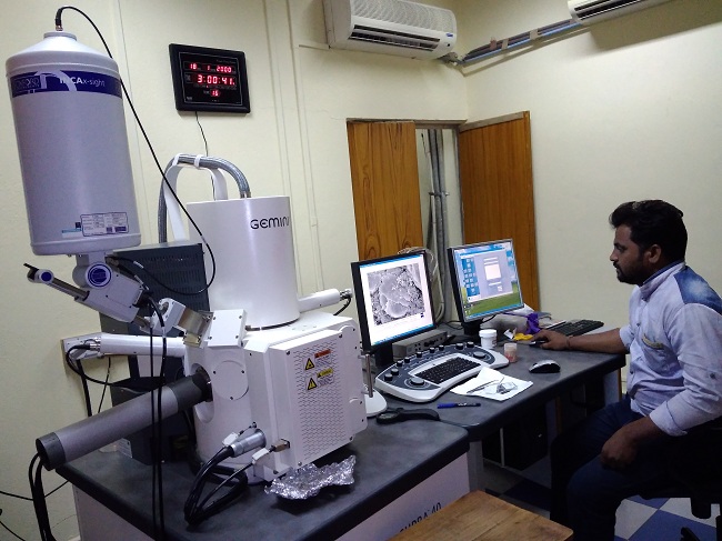
Field Emission Scanning Electron Microscope
Objective
Electron Microscopes are indispensable tools for today's nano technology,development and production. Field Emission Gun Scanning electron microscopes (FEG-SEM) deliver high resolution surface information and are widely used in many application fields such as:
- Materials analysis
- Life Science
- Semiconductor technology
- Quality assurance
The addition of analytical detectors enables full nano structural analysis. The SUPRA™ series, based on the 3rd generation GEMINI® column, offers a complete range of ultra high resolution FE-SEM models to cover all fields of applications in nano technology, cryo, nano structural materials analysis and semiconductor development and failure analysis.
Field Emission Scanning Electron Microscope
Specification of the Instrument:SUPRA 40 Field Emission Scanning Electron Microscope
Manufacturer details:Carl Zeiss SMT AG(Germany)
Purchase source (funding):SCM
Year of installation:2007
Essential Specifications |
|
Magnification |
12-10,00,000 x |
Emitter Thermal field emission type Acceleration Voltage |
1.5-30kV |
Probe Current |
4 pA-10nA(40 nA Optional) |
Standard Detectors |
ZEISS High efficiency In-lens detector
|
Operations |
High Magnification particle analysis
|
Utility and Working Principal
FESEM is the abbreviation of Field Emission Scanning Electron Microscope. A FESEM is microscope that works with electrons (particles with a negative charge) instead of light. These electrons are liberated by a field emission source. A field-emission cathode in the electron gun of a scanning electron microscope provides narrower probing beams at low as well as high electron energy, resulting in both improved spatial resolution and minimized sample charging and damage. For applications that demand the highest magnification possible, it also offers In Lens SEM.The object is scanned by electrons according to a zig-zag pattern. A FESEM is used to visualize very small topographic details on the surface or entire or fractioned objects. Researchers may apply this technique to observe structures that may be as small as 1 nanometer (= billion of a millimeter). The FESEM may be employed for example to study organelles and DNA material in cells, synthetical polymeres, and coatings on microchips.
Sample Details
- Solid samples e.g., Metallic, Amorphous, coated sample or thin films etc.
- Dimension: 10x10mm or larger
- Powder and Liquid samples are not allowed
Field emission scanning electron microscopy (FESEM) provides topographical and elemental information at magnifications of 10x to 300,000x, with virtually unlimited depth of field. Compared with conventional Scanning Electron Microscope(SEM) field emission SEM (FESEM) produces clearer, less electrostatically distorted images with spatial resolution down to 1 1/2 nanometers – three to six times better.
Other advantages of FESEM include:
- The ability to examine smaller-area contamination spots at electron accelerating voltages compatible with Energy Dispersive Spectroscopy (EDS).
- Reduced penetration of low-kinetic-energy electrons probes closer to the immediate material surface.
- High-quality, low-voltage images with negligible electrical charging of samples (accelerating voltages ranging from 0.5 to 30 kilovolts).
- Essentially no need for placing conducting coatings on insulating materials.
- Advanced coating thickness and structure uniformity determination
- Small contamination feature geometry and elemental composition measurement