- APPLY FOR SLOT
- Internal Users
- External Users
- SLOT BOOKING STATUS
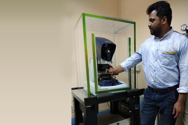
3D - Optical Surface Profilometer Laboratory
Phone : 91-3222-269934
Location : NB / FF / 3, CRF
Facilitator :
Prof. Jyotsna Dutta Majumdar, Metallurgical & Materials Engineering
Email: jyotsna@metal.iitkgp.ernet.in, Contact:+91-3222-283288
For Internal Users - Click Here to apply for Slot
For External Users - Click Here to apply for Slot
Objectives
To measure the surface profile in order to quantify its roughness critical dimensions as step, curvature, flatness from the surface topography.
People

Prof. Jyotsna Dutta Majumdar
Facilitator
Metallurgical & Materials Engineering
jyotsna@metal.iitkgp.ernet.in
+91-3222-283288
Equipment Details
3D-Optical surface profilometer
Manufacturer- Bruker
Model- Contour GT
Year of Installation- 2014
| Specifications | |
| Max. Scan Range | Up to 10 mm |
|
RMS Repeatability (PSI) |
0.02 nm* |
| Lateral Resolution |
0.38 μm min (Sparrow criterion); 0.26 μm (with AcuityXR®) |
| Step Height Accuracy | < 0.75%** |
| Step Height Repeatability | < 0.1% 1 sigma repeatability |
| Max Scan Speed | 47 μm/sec (with standard camera) |
| Sample Reflectivity | 0.05% - 100% |
| Max. Sample Slope |
Up to 40° (shiny surfaces); Up to 87° (rough surfaces) |
| Sample Height | Up to 100 mm (4 in.) |
| Sample Weight | Up to 4.5 kg (10 lb) |
| XY Sample Stage | 150 mm (6 in.) manual or automated option |
| Tip/Tilt Function | ±6° manual in stage |
| Optical Metrology Module |
Patented dual-LED illumination; Single-objective adapter; Optional automated or manual turret; Single or auto FOV lenses |
| Objectives |
Parfocal: 2.5x, 5x, 10x, 20x, 50x, 115x LWD: 1.5x, 2x, 5x, 10x TTM: 2x, 5x, 10x, 20x Brightfield: 2.5x, 5x, 10x, 50x |
| Available Zoom Lenses | 0.55x, 0.75x, 1x, 1.5x, 2x |
| Camera |
Standard monochrome: 640 x 480 High-resolution monochrome (option): 1280 x 860 Standard color (option): 640 x 480 High-resolution color (option): 1280 x 860 |
| Software System |
Vision64 Control and Analysis Software on Windows 7 64-bit OS |
| Software Packages |
Production interface; Acuity XR; Annular Analysis; High Speed AF; Optical Analyses; Advanced Image |
| XY Automation |
Manual stitching standard; Automated stitching, scatter and grid automation standard with motorized XY stage |
| Calibration- | Via traceable step standards |
| System Footprint | 450 mm (W) x 534 mm (D) x 632 mm (H) |
| System Weight | 60.3 kg (133 lb) |
Utility and Working Principal
Optical profiling uses the wave properties of light to compare the optical path difference between a test surface and a reference surface. Inside an optical interference profiler, a light beam is split, reflecting half the beam from a test material which is passed through the focal plane of a microscope objective, and the other half of the split beam is reflected from the reference mirror. When the distance from the beam splitter to the reference mirror is the same distance as the beam splitter is from the test surface and the split beams are recombined, constructive and destructive interference occurs in the combined beam wherever the length of the light beams vary. This creates the light and dark bands known as interference fringes.
Since the reference mirror is of a known flatness – that is, it is as close to perfect flatness as possible – the optical path differences are due to height variances in the test surface. This interference beam is focused into a digital camera, which sees the constructive interference areas as lighter and the destructive interference areas as darker. In the interference image (an "interferogram") below, each transition from light to dark represents one-half a wavelength of difference between the reference path and the test path. If the wavelength is known, it is possible to calculate height differences across a surface, in fractions of a wave. From these height differences, a surface measurement – 3D surface map, is obtained.
Sample Details
- Metallic, coated sample, thin films
- Dimension 10x10mm or larger
- Preparation No polishing is required

3D Surface contour of Electron beam welded pure niobium sample